ECE492 Section 1 Notes
Welcome! Notes for Spring 2022 Electronic Circuits course. Will make this more pretty as things evolve.
My goal is to make Electronic Circuits so easily digestible, you could teach a middle schooler. We'll see if this works.
Prologue
Hey how are you. I will insert something here later. :)
Section 1.1
We first need to consider the following materials:
- Conductors
- Insulators
- Semiconductors
Consider the concept of the charge for Oxygen (O):
- 8 protons around the nucleus
- 8 electrons (two on the inner orbit, 6 on the outer orbit).
Let's look at the outer most orbit in context with a conductor:
- There are two bands: valency and conduction.
- Electrons are always in the valency band.
- In between, there is an energy gap, which is approximately 0 (meaning electrons can move freely between valency band and conduction band).
- That is the reason why conductive materials act as they do.
Let's look at the outer most orbit in the context of insulators:
- There are two bands: valency and conduction.
- Electrons are always in the valency band.
- In between, there is an energy gap, which is very high (meaning electrons have a very hard time moving between the valency band and conduction band).
- That is the reason insulators, are well, insulators (or their property is insulative).
Let's look at the outer most orbit in the context of semi-conductors:
- There are two bands: valency and conduction.
- Electrons are always in the valency band.
- In between, there is an energy gap, which is exactly 1.12eV (1eV = 1.602 * 10-19J).
- Once electrons are in the conduction band, the semi-conductor will act as a conductor.
This entire class is based on semi-conductor materials.
What is a semiconductor?
It sometimes allow current, and sometimes it doesn't.
Semi-conductors only have 4 electrons in its outermost orbit.
- Carbon
- Silicon
- Germanium
- Lead
What's the best two?
- Silicon and Germanium
Consideration of Silicon:
- Silicon will acquire other silicon atoms to form a covalent bond.
Now let's take a Silicon atom:
- Take a pure silicon atoms and put energy to them: go from insulator to conductive properties, and electrons from the furthest orbit detach and jump to another position.
- When electrons detach, it leaves a hole where it once was, that is viewed as a positive charge for clarity.
Doping: Adding impurity to a pure semiconductor material.
- Tri-Valent Impurity: majority of "holes" (positive charge), also know as P-type semiconductor.
- Penta-Valent Impurity: majority of electrons, also known as N-type semiconductor.
Let's take Aluminum for Tri-Valent example:
- Pair the Aluminum with Silicon atoms, knowing that Aluminum has an outer electron count of 3.
- Silicon will be bounded to the three outer Aluminum electrons, but 1 Silicon will be left.
Let's try Phosphorous for Penta-Valent example:
- Pair Phosphorous with Silicon atoms, knowing that Phosphorous has an outer electron count of 5.
Now what is P-N Junction? It's a diode.
- A P-type semiconductor connected to an N-type semiconductor.
- Recall that P-type just has a lot of "holes" (positive).
- Recall that N-type has a lot of electrons (negative).
- Shouldn't these holes and electrons combine? Electric field is present due to electrons on the N-type side of the P-N junction. This electric field does not allow for combining.
- There is an anode and a cathode on the P-type and N-type side respectively. A diode can be represented with A -> C.
- Now let's connect a battery on each side of the junction, and we supplement 0.5V.
- The electric field barrier becomes thinner and thinner, but not completely gone.
- Now apply 1.0V, the electrons and holes will push against the junction.
Now consider a reverse biased diode:
- A diode where the energy source charge is reverse from the P-N junction.
- Holes to negative and electrons to positive.
Important consideration: A P-N Junction (diode, or biased/reversed biased diode) allows current in only one direction.
What are the V-I characteristics of the P-N Junction/Diode:
- What is PIV? Peak Inverse Voltage.
- Consider the graph below for a typical V-I characteristic of a diode.
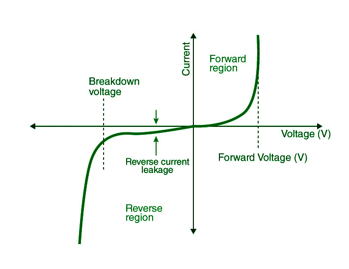
Therefore, important considerations added for P-N Junction diode:
- A P-N Junction (diode, or biased/reversed biased diode) allows current in only one direction.
- Acts like a closed switch in forward biased condition.
- Acts like an open switch in reversed biased condition.
Now consider the following example: Find the current passing through each diode.
- We'll need to break the problem apart.
- Current always flows from higher potential to lower potential.
- Assume ideal diode.
Let's break the problem down:
- Step 1: Fill me in. :)
Insert example 1A
Now let's consider the following example:
- Step 1: Find all possible current flow directions (current always flows from high potential to low potential) and make a determination of whether a diode is open/closed/don't know.
- Step 2: We'll take the assumption that D2 and D3 are closed because we don't know what they are.
- Note: We can't have 3 different voltages at the same node, so our assumption is wrong.
- Step 3: Now we'll verify that our assumption is correct.
- Is D2 and D3 open? Since anode voltage is higher than cathode, then diode acts like a closed switch [in ideal case].
- Therefore, both D2 and D3 are open.
Insert example 1B
Now let's consider this next example.
- Step 1: Find I1, I2, and I3 assuming ideal diodes.
- Find all possible current flow directions (current always flows from high potential to low potential).
- Step 2: We'll assume that
Assignment 1.1
We'll take this and plug it into to find x2:


